×
HOME
PROFILE
LABORATORY
EVENTS
IMPACT
VACANCY
FLAGSHIP
CONTACT
APPLICATION REFINEMENT LABORATORY
Perfecting the solution we provide
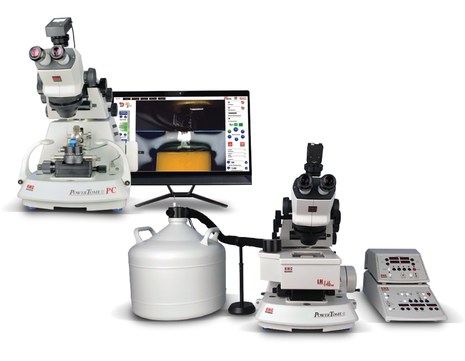
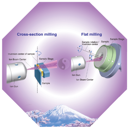
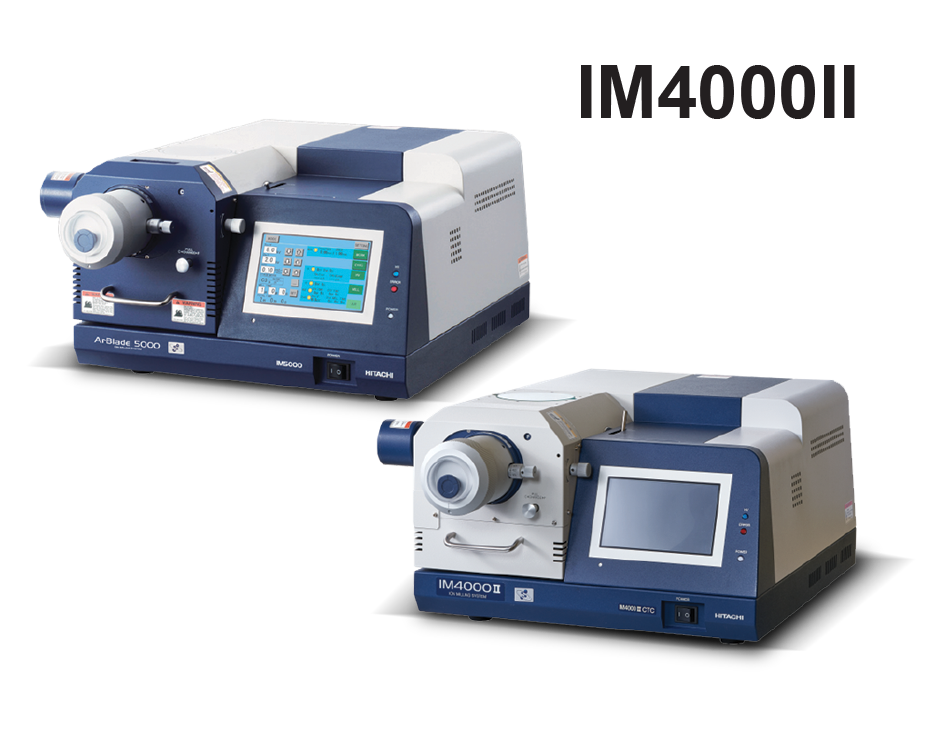
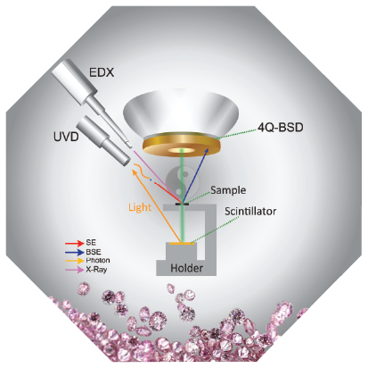
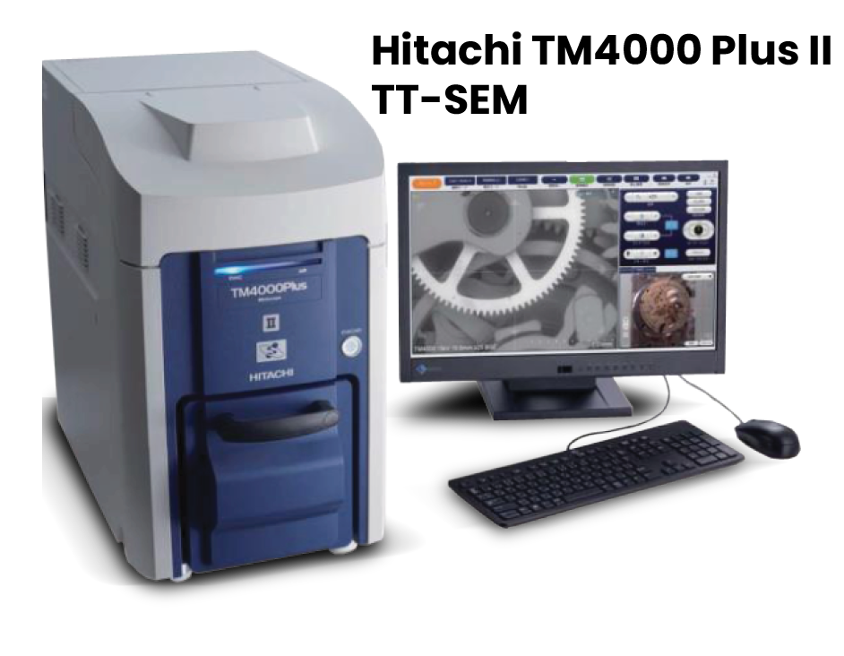
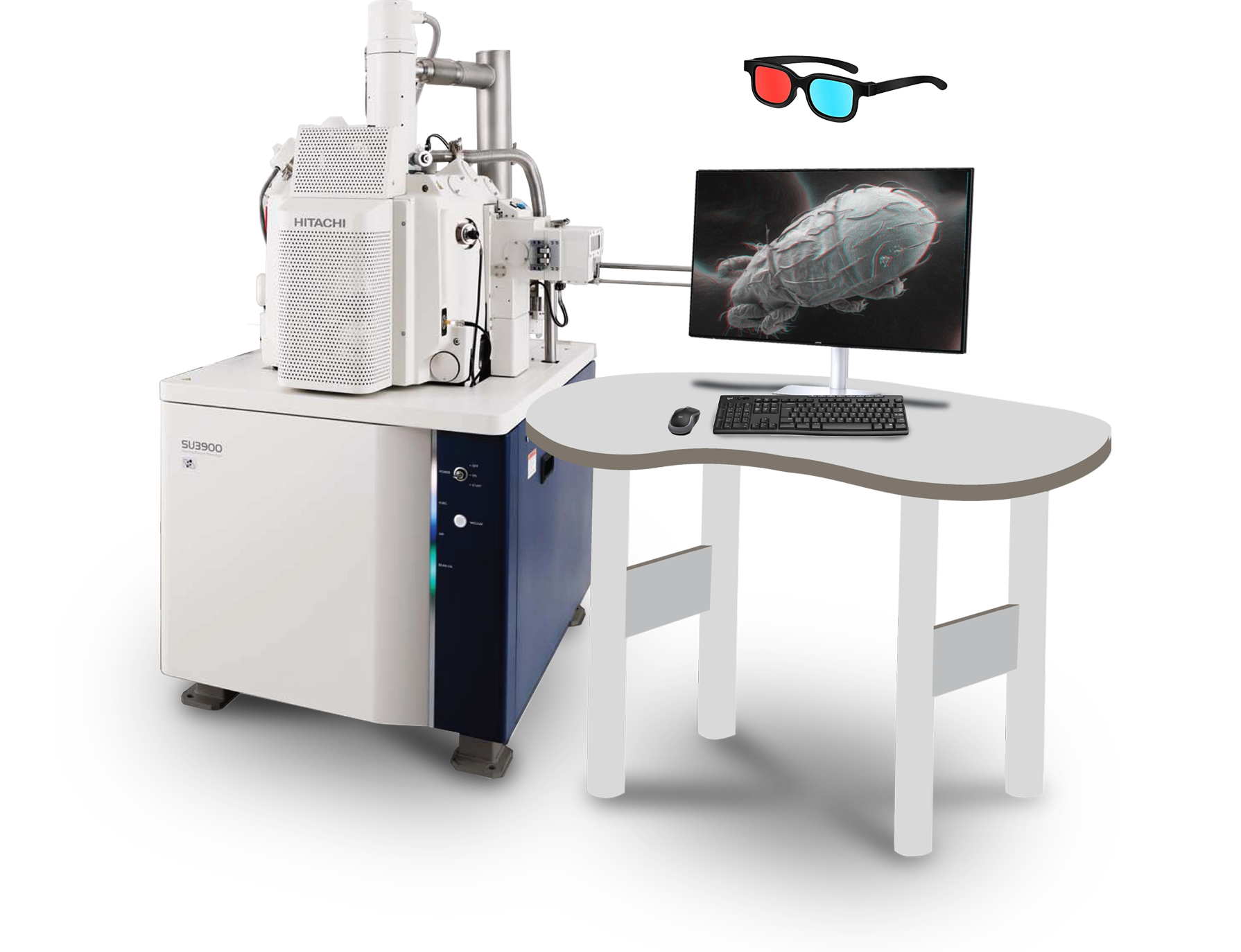
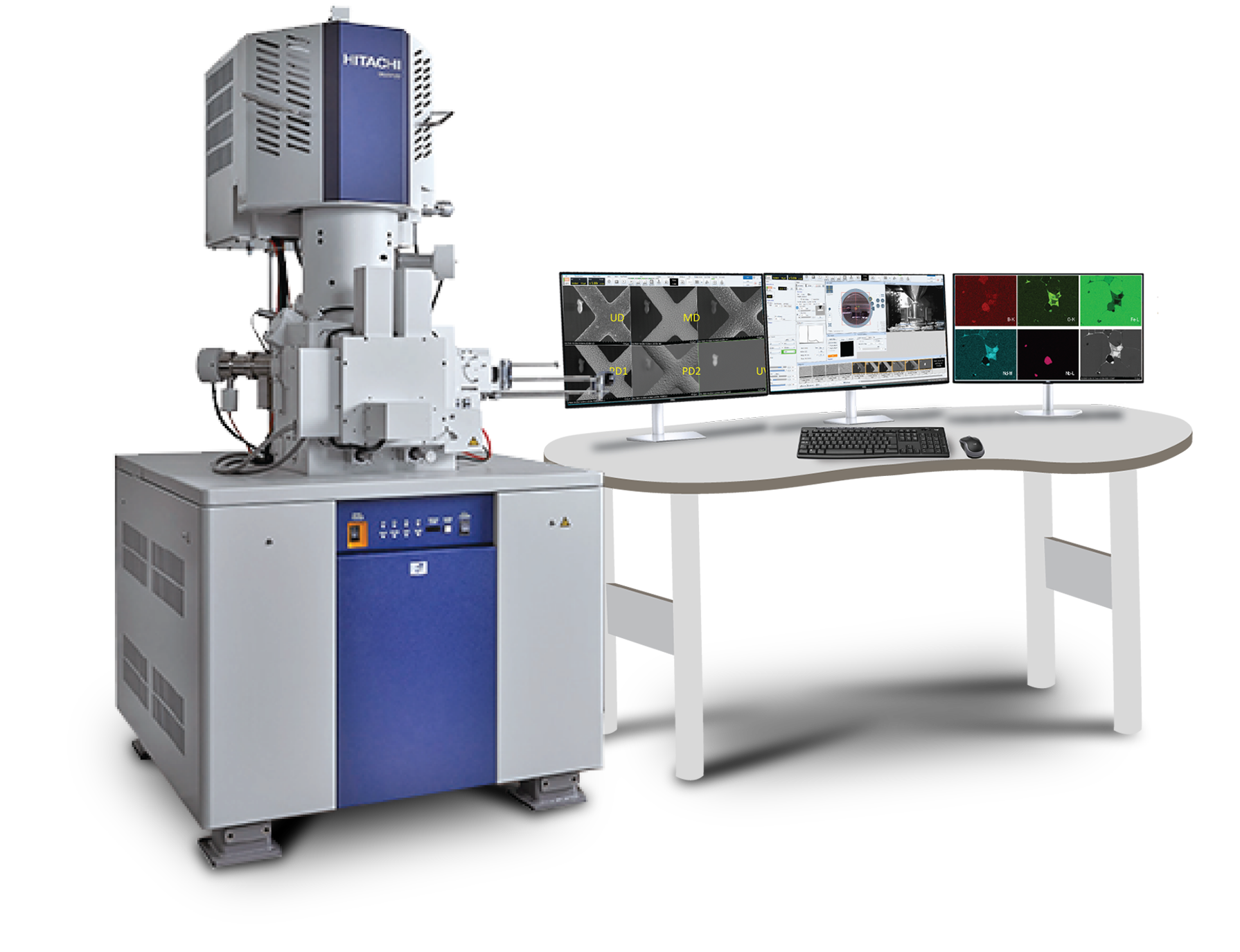
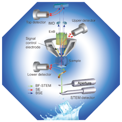
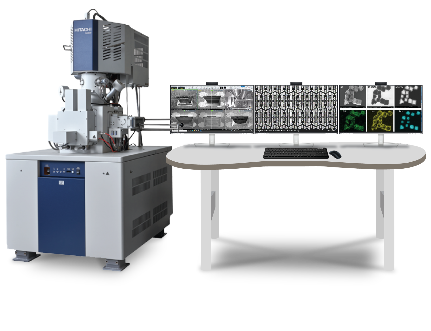
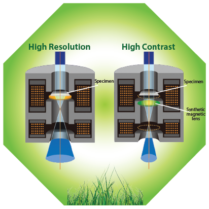
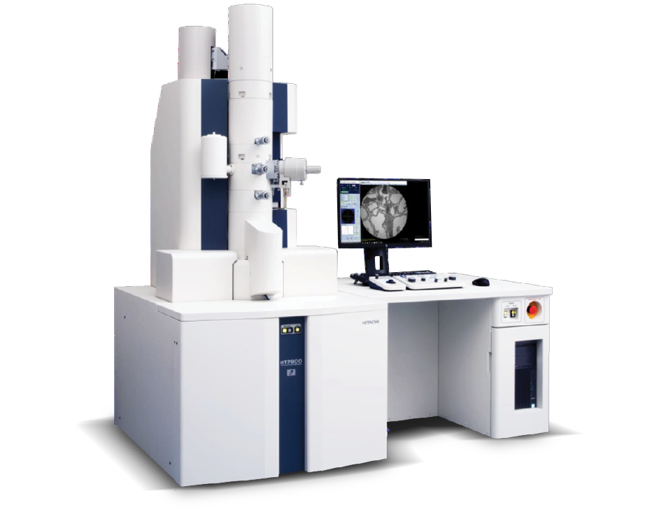
Our Application Refinement Laboratory is constantly updated with the latest state-of-the- art instrumentations to guarantee the ultimate imaging and characterization capability. This is inline with our objective for refining and perfecting every solution we provide to our customers.

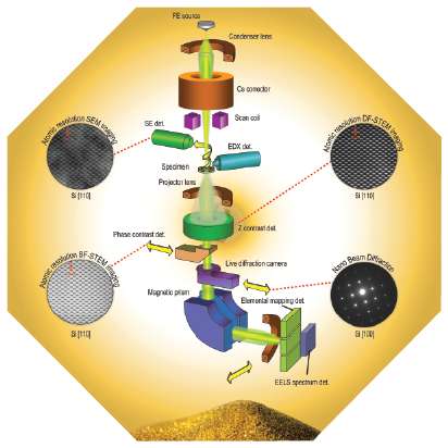
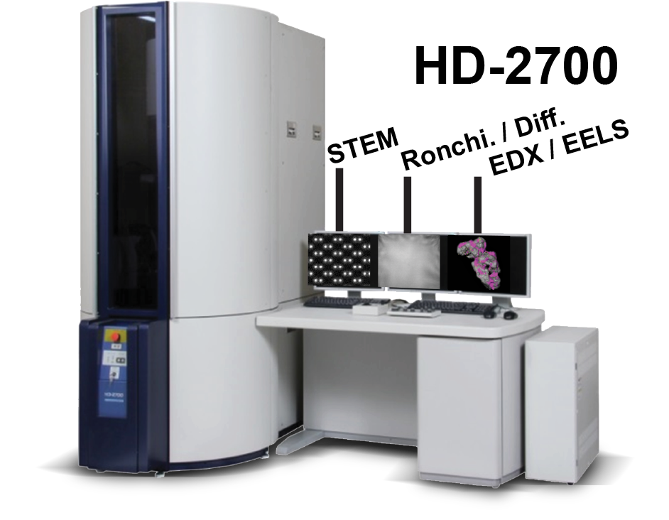
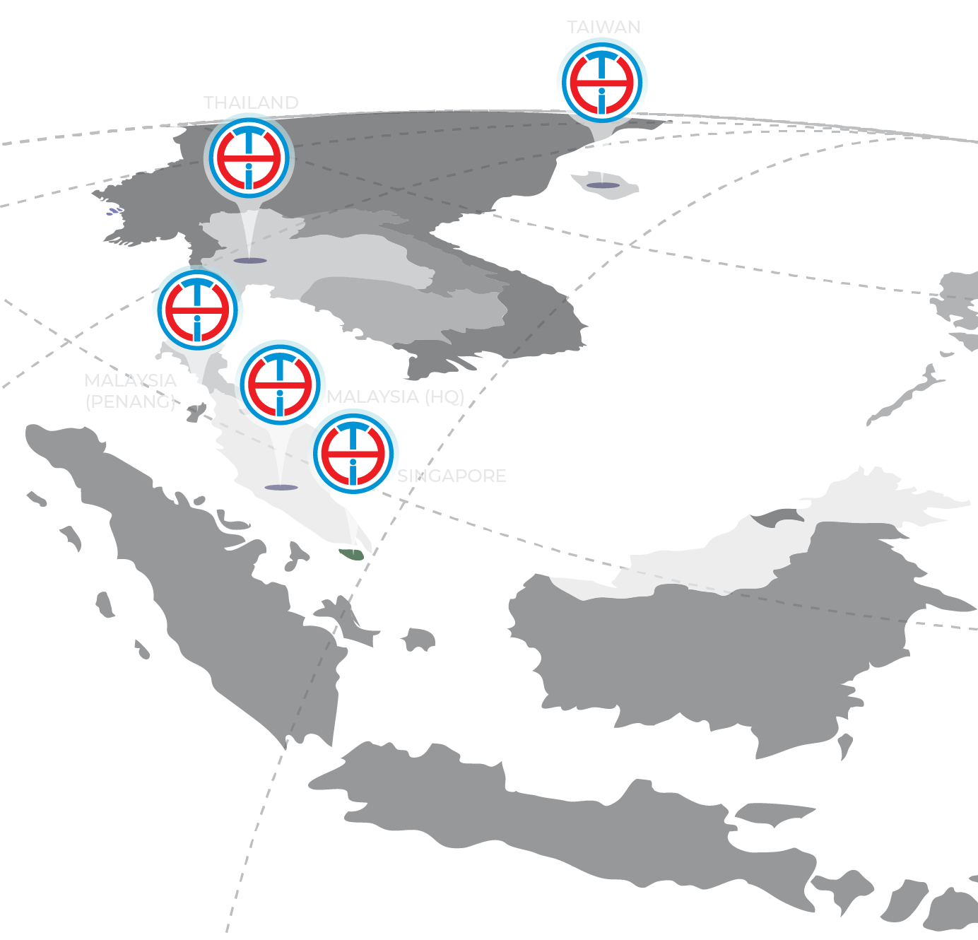
A suite of complementary imaging and characterization tools installed at our head office and branch offices, coupled with highly trained in-house specialists are ready factors for successful collaborations, trainings, workshops and analytical services.
SE 3nm @ 30kV
SE 0.7nm @ 15kV
SE 0.6nm @ 15kV
Atomic lattice 0.24nm @ 100kV
SE 0.1nm @ 200kV
    RT and Cryo-Ultramicrotomy
  • Room temperature and Cyro-sections
  • Thin and ultrathin section preparation
  • Glass knife maker
    Argon Ion Milling
  • Flat milling and x-section milling
  • Compatible holders for SEM
  • Cryogenic cooling
    Tabletop SEM
  • Tabletop SEM
  • UVD for Topo, CL & STEM
  • 4Q-BSED
  • Camera Navigation and SEM-MAP
  • Motorized stage
  • Map 3D and Multi ZigZag
  • Automated Particle analysis
SE 3nm @ 30kV
    Variable Pressure SEM
  • UVD-Topo, UVD-CL, UVD-STEM
  • 5seg-BSED
  • VP up to 650Pa
  • Peltier coolstage
  • Si₃N₄ SDD
  • Camera Navigation and SEM-MAP
  • Map 3D and Multi ZigZag
  • Automated Particle analysis
    Sub-nm Schottky FE-SEM
  • HV, VP and Deceleration modes
  • In-column detectors for all modes
  • UVD & PD-BSED for Compo / Orientation
  • Deceleration mode ( +/-)
  • EDS/t-EBSD @6mm
  • STEM ( BF/DF )
  • Multi ZigZag and SEM-MAP
SE 0.8nm @ 15kV
    Ultrahigh resolution Cold FE-SEM
  • Cold FEG and Semi-in-lens Obj.
  • Pure signal detection ( Super ExB )
  • Extreme surface sensitivity
  • Deceleration optics
  • IMD and OCD detectors
  • Class-leading geometry ( windowless SDD )
  • STEM BF/HAADF
  • Multi ZigZag and SEM-MAP
SE 0.6nm @ 15kV
    Low voltage TEM
  • 20 to120kV LaB6
  • Dual-mode obj. lens
  • HR and HC modes
  • Wide field and whole view
  • 16Mpix CMOS camera
  • Electron diffraction imaging
  • Single and double-axis Tomography
Atomic lattice 0.24nm @ 100kV
    Cs-corrected SEM/STEM
  • 120 and 200kV FEG
  • Cs-corrector
  • Atomic resolution SEM
  • Atomic resolution BF-STEM
  • Atomic resolution ADF-STEM
  • Nano-beam diffraction ( NBD )
  • Fitted with EDS and EELS
SE 0.1nm @ 200kV
    RT and Cryo-Ultramicrotomy
  • Room temperature and Cyro-sections
  • Thin and ultrathin section preparation
  • Glass knife maker
    Argon Ion Milling
  • Flat milling and x-section milling
  • Compatible holders for SEM
  • Cryogenic cooling
    Tabletop SEM
  • Tabletop SEM
  • UVD for Topo, CL & STEM
  • 4Q-BSED
  • Camera Navigation and SEM-MAP
  • Motorized stage
  • Map 3D and Multi ZigZag
  • Automated Particle analysis
SE 3nm @ 30kV
    Variable Pressure SEM
  • UVD-Topo, UVD-CL, UVD-STEM
  • 5seg-BSED
  • VP up to 650Pa
  • Peltier coolstage
  • Si₃N₄ SDD
  • Camera Navigation and SEM-MAP
  • Map 3D and Multi ZigZag
  • Automated Particle analysis
SE 0.7nm @ 15kV
    Sub-nm Schottky FE-SEM
  • HV, VP and Deceleration modes
  • In-column detectors for all modes
  • UVD & PD-BSED for Compo / Orientation
  • Deceleration mode ( +/-)
  • EDS/t-EBSD @6mm
  • STEM ( BF/DF )
  • Multi ZigZag and SEM-MAP
SE 0.6nm @ 15kV
    Ultrahigh resolution Cold FE-SEM
  • Cold FEG and Semi-in-lens Obj.
  • Pure signal detection ( Super ExB )
  • Extreme surface sensitivity
  • Deceleration optics
  • IMD and OCD detectors
  • Class-leading geometry ( windowless SDD )
  • STEM BF/HAADF
  • Multi ZigZag and SEM-MAP
Atomic lattice 0.24nm @ 100kV
    Low voltage TEM
  • 20 to120kV LaB6
  • Dual-mode obj. lens
  • HR and HC modes
  • Wide field and whole view
  • 16Mpix CMOS camera
  • Electron diffraction imaging
  • Single and double-axis Tomography
SE 0.1nm @ 200kV
    Cs-corrected SEM/STEM
  • 120 and 200kV FEG
  • Cs-corrector
  • Atomic resolution SEM
  • Atomic resolution BF-STEM
  • Atomic resolution ADF-STEM
  • Nano-beam diffraction ( NBD )
  • Fitted with EDS and EELS